Bienvenidos

Jahir te da la bienvenida al blog de semiconductores organicos. Espero te sea util!

sábado, 17 de julio de 2010

RFIC (radio frequency integrated circuit)

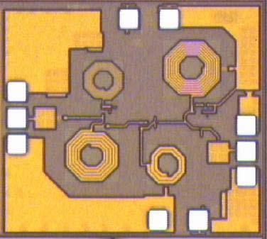
Los RFIC (del inglés radio frequency integrated circuit) son circuitos integrados que trabajan en el rango de ondas de radiofrecuencia.

La electrónica actual tiene una fuerte tendencia al empleo de las tecnologías inalámbricas, en las cuales se conjuga toda la potencialidad del procesado digital y analógico, para altas frecuencias, en un mismo sistema. Estos sistemas integrados requieren bajo coste, bajo consumo, altas prestaciones y tamaño reducido, en donde el papel que juega la tecnología CMOS es vital para la expansión de los sistemas inalámbricos.
 

Historia

En los últimos años la tecnología CMOS ha evolucionado notablemente logrando mejoras en los niveles de integración y velocidad de proceso. Esto aunado a su bajo coste ha permitido la integración de procesadores digitales junto con el procesado analógico de la señal, dando lugar a la implementación de circuitos integrados de modo mixto. Por su parte, los circuitos integrados de Radio Frecuencia (RF) han sufrido un explosivo crecimiento por su extensa aplicación en sistemas de comunicación y equipos inalámbricos. Con respecto a los problemas tecnológicos, que se derivan de la implementación de estos sistemas en tecnología CMOS, cabe destacar el trabajo realizado por Thomas H. Lee. A él se le deben numerosas contribuciones teóricas de tecnología y diseño en este campo.

Circuitos Activos y Pasivos de Microondas

Los circuitos de microondas están divididos en dos grandes grupos: circuitos activos y circuitos pasivos. Los circuitos pasivos no agregan potencia a la señal que reciben, mientras que los activos sí que pueden agregarla. Los circuitos pasivos incluyen desde elementos discretos como resistencias, inductancias y capacitancias hasta circuitos mas complejos, tales como: Filtros, divisores,combinadores, duplexores, circuladores, atenuadores, líneas de transmisión... Entre los circuitos que pueden ser tanto activos como pasivos, están las antenas, multiplexores, mezcladores... Dentro de los circuitos activos se encuentran los RFICs, diodos, MMICs, receptores, moduladores, osciladores...

La clave la integración

Los sistemas de comunicación inalámbricas transmiten las señales a frecuencias de unos pocos GHz (usualmente entre 1 GHz y 3 GHz); en estas bandas operan sistemas y servicios cuyo impacto es significativo (Bluetooth, 2,4 GHz; UMTS, GPS, DECT, etc).

La demanda actual de estos equipos se ha satisfecho mediante sistemas MCMs, o fundamentalmente, con circuitos, tanto integrados como discretos montados sobre PCBs, basados ambos en tecnologías III-V maduras. El principal problema del uso de estos circuitos es el alto coste y el bajo volumen de producción, es muy limitado. Sin embargo, las necesidades del mercado exigen componentes de radiofrecuencia (RF) pequeños, baratos, de bajo consumo y producción masiva. De modo que los grupos de investigación y, en especial, las empresas de diseño y fabricación de sistemas para RF enfocan sus líneas de investigación para desarrollar circuitos integrados estándar de silicio: CMOS y BiCMOS. Por tanto, los dispositivos activos en estas tecnologías alcanzan las frecuencias requeridas con unas dimensiones muy pequeñas; pero surge un nuevo problema, no se dispone de inductores de calidad.

Esta carencia anteriormente citada es muy restrictiva, pues implica la adaptación de las redes a altas frecuencias mientras que no es necesario, si se está trabajando con bajas frecuencias (por ejemplo, la utilización de circuitos de adaptación de impedancia compleja). Los inductores de calidad, son componentes pasivos y necesarios para muchas otras funciones, como la polarización de transistores en amplificadores de bajo ruido (LNA) o la implementación de tanques LC (circuitos resonadores sintonizados) en osciladores. Otros componentes además de los inductores de calidad, son los varactores integrados que amplíen el rango de valores de la capacitancia sin que ello exija una gran cantidad de área para la integración.

El escalado de la tecnología CMOS (>65nm), ha permitido llegar a la integración en un solo chip de gran capacidad de procesado, comunicaciones inalámbricas (wifi, bluetooth), memoria, video, circuitos de RF, audio. Estos RFIC nos permiten disponer de terminales móviles que integran en un solo chip tecnología cuatribanda, cámara de fotos, navegador de internet, reproductor mp3, reproductor de video, agenda, etc 


Bluetooth es un estandar de conectividad wireless que provee comunicaciones de voz y datos de bajo coste para enlazar teléfonos móviles PDA, PC, cámaras digitales y otros dispositivos portátiles. Está tecnología trabaja a 2.4 GHz. Los dispositivos Bluetooth operan en tres clases de potencia. La clase 2 opera a 0 dBm, la clase 2 opera a 4 dBm y la clase 1 opera a 20 dBm. Todas ellas transmite datos a 1 Mbps y la última generación oscila entre 2 y 12 Mbps
Por lo tanto estos dispositivos deben ser capaces de controlar la potencia desde 20 dBm hasta 0 dBm, Bluetooth habilita este control de potencia optimizándola con LMP (Link Manager Protocol). Consiste en medir la señal recibida (RSSI) y reportando si la señal debe ser amplificada o no. Bluetooth además es considerado un estandar de bajo coste, y lo consigue gracias a la tecnología CMOS. CMOS es usado en esta tecnología como amplificadores de potencia, a continuación se muestra un esquema de un amplificador de este tipo
  
Problemas de diseño

 La integración de la sección digital y de RF sobre un mismo sustrato es un tema de gran interés en la actualidad por las diferentes dificultades que ello conlleva. La problemática de la integración de estas dos secciones tan diferentes repercute en todos los niveles de abstracción y flujos de diseño, desde el desarrollo de la arquitectura, particionado, simulación, pruebas, elección de estándares, normativas, algoritmos, protocolos de comunicación, pasando por aspectos de simulación (CAD y modelado) para la planificación y coordinación de flujos de diseño (en sus diferentes niveles de abstracción), todos estos aspectos enmarcados y delimitados por el desarrollo de la tecnología actual y futura. Por lo tanto, a pesar de las ventajas, es innegable que la tecnología CMOS sufre de una serie de limitaciones, de entre las cuales se destacan los problemas referentes a la integridad de la señal. De entre estos problemas, el ruido de conmutación puede ser considerado un factor crítico en el diseño de Circuitos Integrados. La actividad eléctrica de los nodos digitales se acopla desde la red de distribución de energía al sustrato, implicando la transmisión de ruido a puntos sensibles de las secciones analógicas o de radiofrecuencia (RF), lo cual degrada notablemente sus prestaciones

Aplicaciones
Las principales aplicaciones de los circuitos integrados de radiofrecuencia son los productos para comunicaciones inalámbricas, como por ejemplo, teléfonos móviles y PCS (servicio de comunicaciones personales: conjunto de tecnologías digitales celulares), estaciones base, redes de área local inalámbricas y módems para televisión cable.


Publicado por: Jahir Alonzo Linares Mora C.I: 19769430 CRF
Bibliografia: http://es.wikipedia.org/wiki/RFIC

Passives for RF design

(Passives for RF Design) Designers can choose from fully integrated systems or fully discrete solutions with their associated pros and cons. Both thin film and PMC are rapidly developing technologies, and a number of new devices will soon be emerging. The PMC process is ideal for integration of the passive content of the RF circuit to optimize PA or LNA performance for a given application.

Radio continues to be one of the most powerful technology drivers in microelectronics with many evolutionary changes taking place in the last few years. Consumer and mission-critical applications require solutions that are smaller, increase functionality and reliability, and improve signal clarity, while attaining lower power consumption.

To achieve this, almost all modern radios now use digital modulation schemes instead of standard analog. This also fits with the trend of higher frequencies to make use of the wider bandwidth required for these applications. The higher-frequency designs also drive to smaller physical layout because the shorter wavelengths can be accommodated in much smaller packages (i.e., the wavelength at 5.8 GHz is nearly 6.5 times smaller than at 900 MHz).

Although radio design continues to evolve with increasing complexity and need for security, the actual radio block diagram has remained virtually unchanged.

Figure 1 is a block diagram of a dual-conversion super-heterodyne transceiver, one of the most common radio design schemes used today. However, the direct-conversion (zero intermediate frequency) receiver is gaining momentum. The direct-conversion receiver has a single mixing stage that converts the received signal directly to baseband and reduces the cost considerably — at the expense of performance.

Figure 1. Basic super heterodyning transceiver.

The basic radio consists of several key components, and each has a specific job in the chain: antenna, switch, low-noise amplifier (LNA), filter, mixer, oscillator, modulator/demodulator. As the applications have evolved, so has the component technology that has enabled major downsizing of these elements to take place.

Early radio designs were necessarily based on discrete passive components designed for high-frequency performance. These use low-loss, high-frequency dielectrics (NP0 ceramic, porcelain or glass), but require precious metal electrode systems that can withstand the high firing temperatures associated with ceramic material processing and still provide good conductivity. These devices remain a suitable solution for high-power RF applications but are nearing the limit of downsizing for microcircuit applications.

LTCC technology

The next stage of evolution came with low-temperature co-fired ceramic (LTCC) technology. This technology enables integration of passive components within compact modules and can provide a platform for actives. This integrated technology does yield small size but requires careful design discipline to achieve repeatable characteristics. LTCC is essentially a “wet” or tape process technology: Material is screened in place, building up the device layers, while the lower temperature manufacturing process enables the use of more standard conductive metals such as copper for internal electrodes and contacts. Plated-through vias are used for interlayer interconnection, and the electrical conductors can be configured in plates (capacitors) or spirals (to make efficient inductors). Different low-temperature ceramic materials with a variety of characteristics are available, including high-capacitance density dielectrics, but these yield high-dielectric constant at the expense of tighter temperature and voltage coefficients that characterize the high-temperature ceramic types.

This type of lay-down process also has wider process tolerances (from the capability of the wet system to the variability of post-firing shrinkage) with interconnect line widths limited to ~150 microns. Table 1 gives comparative data for key characteristics. The technology is applicable to the passive and active modules, such as power amplifiers (PAs), RF switches, and RF front-ends by integrated capacitors, resistors, and inductors in a small area. The process results in a mechanically strong and compact structure but does limit the materials available for RF component design.

One challenge facing designers working with LTCC is the ability to characterize the RF properties of the complex internal structures that lack electrical models. Most embedded components, especially spiral inductors and parallel plate capacitors, suffer from significant parasitic coupling due to their large area and proximity to other structures or to ground planes.

It follows that LTCC modules are more suited to application-specific designs in high-volume platforms, as varying the design for different configurations becomes more problematic as their complexity increases. This technology also benefits from economies of scale — once upfront costs for custom design and characterization have been met, the process itself can support low-cost manufacturing — but it also limits any future revisions and changes without a module redesign.

Because LTCC technology in itself is not always the optimum performance solution, there has been an increased interest in new integrated devices that have evolved from discrete solutions based on thin film technology.

Thin film solutions

Thin film technology, as a first step, goes back to a discrete format. The key difference with this technology is that it is based on photolithography and plasma-enhanced chemical vapor deposition (PECVD) processing. The photolithography gives extremely precise geometry, while the low-temperature PECVD process combines the benefits of high conductivity conductors with the use of highly stable dielectrics (e.g., SiO2) deposited on a stable alumina base. The technology also allows downsizing to 0201 size and further integration. The most basic element is the thin-film capacitor as shown in Figure 2.
Figure 2. Thin-film capacitor structure.
 
The system above is characterized by stable dielectric, single-layer construction, which eliminates harmonics, is readily modeled and is reproducible. Designs breadboarded on the bench will be precisely reproduced in mass production at the CEM, month to month and year to year. Because the parts are discrete circuit elements, there are no up-front design costs and full design flexibility is maintained throughout the program lifetime. Ultra-stable dielectrics usually have a trade off: low dielectric constant. But thin film is capable of far thinner dielectric films (~1 µm) compared to LTCC (50 µm to 250 µm), which results in a higher cap yield per mm2. The conductors used for the electrodes also have lower resistivity (~1 m▸/mm2) than their LTCC counterparts (10 - 20 m▸/mm2), giving greater RF power-handling capability. Because of their precision, these devices can be used in conjunction with LTCC packages, while any given LTCC module will have limited design flexibility. The small size and termination compatibility of discrete thin film devices means that they can be used to fine-tune an application or modification or tuned last-minute for Federal Communications Commission (FCC) compliance.

Figure 3 shows how these components are typically configured in a standard radio application.

Figure 3. Key design areas for thin film technology.

The LNA is one of the more critical sections in the receiver circuitry. To maximize the performance, it is essential to have stable biasing and accurate impedance matching. Thin film provides discrete capacitors and inductors with high Q, low equivalent series resistance (ESR), and accurate capacitance values (±.01 pf) and inductance values (±.1 nH).

By using this technology, a low-noise amplifier (LNA) can have a more accurate match over temperature and greater repeatability from board to board compared to both traditional discrete devices and wider-tolerance LTCC.

Figure 4a shows the deviation in S11 when comparing NP0 multilayer ceramic capacitor (MLC) vs. thin film capacitors. Notice that the thin-film capacitor response tracks with no variation between parts. This demonstrates exactly how precise the thin-film process can be from capacitor to capacitor and from batch to batch. This not only improves the quality of the LNA, it can actually improve the yield in manufacturing by eliminating the fine-tuning of circuits in production. Figure 4b shows the response at higher frequencies. Being single-layer devices, thin film shows no harmonic resonances.

Figure 4. Thin film vs NP0 MLC ceramic.

The same components can be used to accomplish the critical matching of the input and output of a power amplifier. By using low-loss, thin-film capacitors and inductors, more power can be sent to the amplifier transferred to the antenna. This results in improved performance and increased efficiency of the power amplifier, as well as improved temperature performance.

Antenna matching is also a critical design issue. The available real estate for the antenna is continually decreasing, which generally leads to a non-ideal form-factor design. This situation will almost always require an impedance matching circuit for the antenna. Thin film capacitors and inductors are ideal for this application, providing an accurate match of impedance to the antenna to maximize energy transfer under all conditions to minimize losses from the PA or to the LNA.

Beyond high-accuracy microminiature capacitors and inductors, thin-film PECVD technology also lends itself to integration. By combining both a capacitor and inductor element on the substrate, an inductor and capacitor (LC) low-pass filter (LPF) can be formed, as shown in Figure 5. These can be made in the same small form factors (0402 and up) and so use little board space while saving cost through component count reduction. These thin-film filters provide high out-of-band attenuation (greater than 30 dB) while maintaining the lowest insertion loss available to the RF designer (less than 0.3 dB). They can also be used to isolate the frequency of interest on the output of the mixer after conversion. The filters must be internally matched to 50 ▸ in order to achieve specified performance.

Figure 5. Thin film LPF and response for a 915 MHz LPF.

A directional coupler is a device that samples an RF/microwave signal while minimizing loss to the signal. Thin-film devices, based on back-to-back inductors, produce high-directivity, low-insertion-loss directional couplers. These couplers offer the highest amount of directivity found on the market today, in small package sizes down to 0402. In the diagram in Figure 6, the coupler is being used to sample the output and send the sample to a gain control circuit for the power amplifier. As with the LPF, the couplers are also capable of handling up to 3 W continuous power.

Figure 6. Directional coupler.

Directional couplers work from the principal of field coupling. The electric field produced by a transmission line in series with the signal is coupled onto an adjacent conductor through the air or dielectric medium. Coupler elements can be included within LTCC modules. The technology allows lumped elements, rather than coupled lines, to produce directional couplers to 10 dB. However, thin-film technology has a number of advantages in this area. The finer line widths maximize the coupling coefficient, making available hybrid couplers to 3 dB in 0603 size.

This coupler, with port configuration shown in Figure 7, is designed to couple 3 dB of power to another channel, with the addition of a 90 ° phase shift to the signal. This can be useful in designs using an in-phase and quadrature (I/Q) architecture where the channels are 90 ° out of phase. By using a hybrid coupler on the output of the oscillator, the local oscillator (LO) can be generated for both I and Q sections. It can also be instrumental when using two amplifiers to improve the linearity by splitting the power between the two circuits and then recombining after amplification. This reduces harmonic emissions, improves efficiency and increases gain from an amplifier.

Figure 7. Hybrid couplers used to improve linearity.

The latest stage in evolution is passive microcircuits (PMC). PMC goes to the next level of passive integration. Its key advantages are that it retains the minimum line width capability and line width precision of thin film, but increases the maximum stacking layers capability. This can be used for increased capacitor and resistor density per mm2 and added turn capability in inductor elements. Table 1 gives the prime characteristics for these materials.

The PMC process is ideal for integration of the passive content of the RF circuit to optimize PA or LNA performance for a given application. As with all integration, the higher the complexity, the more single-application specific the device.

In summary, designers have choices at the outset of the product cycle to choose from full integrated systems to full discrete solutions with their associated pros and cons. Both thin film and PMC are rapidly developing technologies, and a number of new devices are guaranteed to be emerging during the next few quarters.

Publicado por: Jahir Alonzo Linares Mora C.I: 19769430 CRF
Bibliografia: http://rfdesign.com/mag/508RFDF2.pdf

Overcoming the RF challenges of multiband mobile handset design

Demands on components in the RF signal chain of a mobile handset increase with the number of bandwidths and modes, especially for the antenna and its switch. The integration capabilities of RF CMOS devices solve many of these issues while maintaining peak performance.

CMOS has long been regarded as the technology of choice for integration, particularly in high-volume applications where cost is a major driver. During the last few years, advances in CMOS technology have led to its use in analog devices, and then into the intermediate frequency (IF) and radio frequency (RF) domains that were once dominated by BiCMOS and GaAs. As the industry drives forward with multiband applications, these developments have come not a moment too soon.
 
The bottom line is that the RF signal path in a mobile handset has become extremely crowded. The complexity of cellular phones has grown at a rapid pace, moving from dual-band, to tri-band, and now quad-band. In addition, these phones also need to handle a variety of signals for peripheral radios, such as Bluetooth, Wi-Fi, and GPS. This trend is expected to continue as WiMAX and LTE (4G) capabilities are added. In a mobile handset, the antenna switch is the gatekeeper that controls antenna access for all of the radio signals. Currently, designers are specifying new single-pole, 9-throw (SP9T) switches, and we can reasonably expect that SP10T is not far away.

RF challenges

Handsets now being developed incorporate tri-band WCDMA and quad-band EDGE platforms, an architecture that demands at least seven radios in a single handset. Most likely, the market will standardize on at least seven bands, with room for an eighth (for LTE). Regardless, complexity will continue to rise due to the increased popularity of peripheral radios and functions that also need access to the antenna.
 
All of this has greatly complicated the RF front-end by more than tripling the number of high-power signal paths engineered in today’s quad-band EDGE handsets. By its nature, a multiband handset must handle numerous RF paths that all operate on different bandwidths. Yet, they all need to access the same antenna. The most effi cient approach is to path all of the signals through a single RF switch.  For switch manufacturers, this has meant a corresponding evolution from single-pole 4-throw (SP4T), to SP7T, to now SP9T confi gurations in order to handle the increased number of signals. Increased functionality also impacts the antenna, which must effectively radiate from 800 MHz to 2200 MHz from a tiny footprint. Antenna designers are addressing these issues by taking advantage of performance-enhancing matching, switching, and lumped tuning elements. Ultimately, though, it is the RF switch that must be capable of switching up to nine paths or more of high-power RF signals with low insertion loss, high isolation, and exceptional linearity. Next-generation designs require to/from fi lter banks, and, as a result, the burden on the switch element is high. In terms of specifi cations, new applications tend to require very low insertion loss due to the signal going through multiple switch paths; very high linearity due to a WCDMA platform; very high isolation for critical paths; and a small, effective switch solution for independent (yet simultaneous) signal paths with up to 14 control states. In a mobile handset, RF designers are typically responsible for the antenna switch module (ASM), front-end module (FEM), and the transmit module. The ASM typically includes a switch, decoder, power amplifi er (PA) low-pass fi lters, ESD circuitry, and a voltage generator.

 Figure 1. Next-generation mobile handset design must handle a multitude of receive and transmit signal paths.

A multimode, multiband mobile handset generally uses a single PA module to handle all of the quad-band GSM/EDGE signals. In contrast, each WCDMA signal requires its own individual PA. Figure 1 shows a next-generation mobile handset design. The orange area shows the additional PAs and filters that are required to handle the multitude of receive (Rx) and transmit (Tx) signal paths.

 A quad-band GSM handset with one WCDMA band requires at least a single-pole, 6-throw (SP6T) switch to manage all of the signal paths. Designers could use a diplexer and two SP3Ts (which is a popular GaAs configuration), but this results in higher insertion loss than when using a single SP6T switch. In all of these designs, a multiband scenario means significant architectural, performance, and cost challenges. And, any design trade offs in a multiband phone still require the handset to meet or exceed the performance levels of all the standards supported.

Insertion loss

Insertion loss is important in multiband designs because it directly impacts the effective power-added effi ciency (PAE) of the PA. GSM PAs are typically run in saturation at up to 3 W, with an average PAE of 55%. The PA is responsible for half of the total current drain in the handset, so any deterioration of efficiency has a direct impact on battery life. Maintaining the PA’s PAE, then, needs to be a high priority. Early multiband WCDMA/GSM handsets featured separate signal chains for WCDMA and GSM that were then pathed to separate antennas. While this worked for prototypes and fi rst-generation designs, market pressures required a more cost-effective, spacesaving approach. Clearly, the industry needed integrated ASMs that handled seven or more signals.

Initially, SP7T switches were used to support handset architecture with one WCDMA and four GSM bands. Later, designs such as the PE42693, a monolithic SP9T, were developed on UltraCMOS process technology. Figure 2 shows insertion loss over frequency for this switch in terms of multiple transceiver (TRx), Tx, and Rx signals. This level of performance is necessary to ensure effi cient RF front-end designs. The SP9T switch is one of the latest advancements in switch architectures. It can be confi gured to handle multiple bands of WCDMA, GSM, and peripheral radios. The switch in Figure 1, for example, is handling three bands of WCDMA, with paths to duplexers and three PA modules. The switch also handles quad-band GSM/EDGE, which has a single PA module associated with it. In effect, this device has to route fi ve highpower signals through a single switch that is controlled by a simple decoder.

Figure 2. The PE42693 SP9T from Peregrine demonstrates TRx insertion loss of 0.70 dB at 850 MHz WCDMA.

Linearity

Adding more bands to the handset has greatly increased the technical requirements of the switch, and the linearity and harmonic requirements of WCDMA have put a large strain on the performance. For instance, a switch is now generally agreed to need a third-order intercept point (IP3) of better than +65 dBm. In previous GSM-only designs, there was no comparable linearity requirement. The increased front-end complexity of newer designs makes this high level of linearity extremely difficult to achieve for an active device on any manufacturing process. However, by leveraging the linearity
advantages of the UltraCMOS process, the monolithic PE42693 SP9T in Figure 1 is able to maintain the +68 dBm IP3 of its SP7T predecessor with third-order intermodulation distortion (IMD3) performance that surpasses the industry specification of -105 dBm. This level of IMD3 performance
reduces the potential for interference within the mobile handset’s radio.

Isolation

As the number of signal paths in the handset has grown, so has the need for better isolation. The number of input/outputs (I/Os) in an ASM dictates the level of isolation required. For instance, a gallium arsenide (GaAs) SP9T typically requires 18 control lines. In addition to making it challenging to route all of these lines in and out of a singular switch device, it is particularly challenging for the five high-power ports that require good linearity and isolation. The more I/Os there are, the more likely it is for wires to couple during use and bond. An UltraCMOS SP9T, such as the one in Figure 3, requires only four control lines, so this issue is less serious. Isolation is important because the coupling and bonding of signals can be detrimental to a multiband handset’s performance. For instance, the PCS1900 transmit band overlaps with the DCS1800 receive band. Without isolation of 35 dB or better, unwanted in-band signals could pass through the filters and desensitize the receiver, which would result in dropped calls.
Figure 3. The monolithic UltraCMOS PE42693 SP9T antenna switch offers 4-pin logic control with integral decoder/driver that facilitates 1.8 V and 2.75 V control

Small switches
 
Despite the need for more switching capability, the real estate budget for the ASM is shrinking in new mobile handset designs. The need for highly integrated, small antenna switches becomes more pressing. New process technologies for multithrow switches and the use of CMOS is allowing unprecedented integration and shrinking footprints.

For instance, a GaAs SP7T measures 2.4 mm2 whereas a comparable SP7T switch design using 0.5 µm silicon-on-sapphire (SOS) with equal or better small- and largesignal performance measures 1.2 mm2, a space savings of an extraordinary 50%. Currently available GaAs E/D pHemt or J-pHemt SP9T switches measure 2.85 mm2. An SP9T manufactured using an UltraCMOS 0.5 µm process measures 1.87 mm2 and does not require off-chip ESD devices or linearity enhancing matching components. A 0.25 µm UltraCMOS process is in the final stages of deployment, which will further reduce the size of the SP9T another 10%. Until recently, SP9T and SP7T switches were only available as wire-bond devices.

Recent process developments have led switch designers to flip-chip mount the switch to a low temperature co-fired ceramic (LTCC) substrate without underfill, eliminating the area previously required for wire bonding. This further reduces the device footprint. Currently, wafer-level chip-scale packaging (CSP) is in development to produce Ultra- CMOS switches that can be handled like a standard surface-mount package. Besides process technologies, another way to reduce the ASM’s footprint is to increase integration, a common roadmap for all integrated devices. When manufactured in UltraCMOS, switches can eliminate the decoder, blocking capacitors, and the diplexer that are required with other non-CMOS switch technologies. Combined with CSP technology, this process can dramatically reduce the size and thickness of ASMs. In addition, inherent ESD tolerance and a monolithic CMOS interface simplify implementation and use. Finally, the high yield of UltraCMOS processes and scalability to additional switch throws provides a roadmap to higher levels of integration
for future generations of handsets.

Monolithic switches
 
The technical requirements of the multimode, multiband GSM/WCDMA handset have exceeded the capabilities of traditional RFIC technologies such as GaAs (Table 1). Most critically affected by these ultrahigh performance specs are the antenna and the RF switch. As multiband architectures have grown, so has the requirement for the number of PAs and associated filters. But, in reality, the technical demand on the PAs has not changed, only the need for more PAs in a handset design. A critical challenge on the path to multiband handsets is finding an extremely efficient method to route all of the RF signals to the antenna—the monolithic switch. Fortunately, advanced CMOS processes are already in place to satisfy the increased demands on components in the RF signal chain of a multiband, multimode mobile handset. The integration capabilities of RF CMOS devices in the form of UltraCMOS RFICs solve many of these issues while maintaining peak performance.

Publicado por: Jahir Alonzo Linares Mora C.I: 19769430 CRF
Bibliografia: http://rfdesign.com/mag/707RFDF4.pdf

domingo, 27 de junio de 2010

Silicon RF capacitors set new standard for precision and stability

Using a proprietary semiconductor process, Vishay Intertechnology introduced the industry's first silicon-based surface-mount RF capacitor family. The result was a new standard for high-precision capacitors (HPC) that raised the bar on stability over a broad range of frequencies as compared to conventional capacitors in low profile packages. In addition, the silicon-based surface-mount HPC RF capacitors offered high Q factors, low equivalent series resistor (ESR) values, low parasitic inductance, tight tolerances, and an ultrahigh self-resonant frequency (SFR). Now, the supplier has released a new member of this family in the miniature 0603 case size.

The high-performance, high-precision HPC0603A features SRF values as high as 13 GHz over a broad capacitance range from 3.3 pF to 560 pF. The E12 values available in this range provide extremely stable operation over a wide range of frequencies from 1 MHz to several Gigahertz. Parasitic inductance is a low 0.046 nH. Meanwhile, according to the manufacturer, HPC0603A devices that offer E24 values are scheduled for release in the near future.

In addition, the new capacitor features high Q factors up to 4157, tight tolerances of ±1% or 0.05 pF, and low ESR values. The silicon process guarantees that every capacitor in the production line is within 1% tolerance, said Tony Troianello, marketing manager at Vishay's Integrated Products. Its construction makes it efficient, thus allowing it to handle up to 90 W without any change in the characteristics of the device, added Troianello. The HPC0603A measures 0.063 inches by 0.031 inches [1.60 mm by 0.80 mm] with a 0.022-inch [0.56 mm] height profile. It is rated for a temperature coefficient of capacitance (TCC) of ±30 ppm/°C over an operating range of -55°C to +125°C. Voltage options of 6 V, 10 V, 16 V and 25 V are available.

The HPC0603A's high capacitance range and relatively compact package enable increases in circuit Q, transmission range and reliability. HPC devices' unique construction (see the figure) reduces parasitics by shortening interconnecting traces on PCBs and improves circuit performance by decreasing the distance between components.

This innovative design brings the new capacitor's SRF frequencies to new highs, enhancing performance and transmission/reception quality during operation at high frequencies. As a result, designers of wireless communications devices such as mobile and cordless phones, GPS systems, VCOs, filter and matching networks, RF modules, and base stations can implement HPC devices to reduce product size — simplifying design and reducing the number of components on the PC board — without sacrificing electrical performance.

To predict end performance using simulation programs, a global model for these capacitors has been developed by Modelithics. Integrated with leading EDA tools, the model shows complete characteristics on a variety of PC boards and substrates. It also provides S parameters for these high-precision capacitors.
Samples of the HPC0603A are available, with lead times of up to 10 weeks for production quantities. Typical pricing for U.S. delivery in high-production quantities is $0.082 for 10-pF devices with a ±2% tolerance.


Publicado por: Jahir Alonzo Linares Mora C.I: 19769430 CRF
Bibliografia: http://rfdesign.com/microwave_millimeter_tech/passive_components/radio_silicon_rf_capacitors/

Exploring advances in microwave and millimeter wave devices

As the demand for higher bandwidth and frequencies in wireless and wirleline applications continues to climb, while cost and size continues to go downward, the need for better performing RF and microwave/millimeter wave ICs, discretes, modules and passive devices is far greater today. Thus, the efforts to improve components from capacitors at one end to millimeter wave monolithic ICs at the other extreme are in full swing. This report looks at some of these developments.

For instance, in the RF and microwave power transistors arena, suppliers continue to tap advances in material science, process techniques, transistor structures, and packaging technologies to drive performance of lateral-diffused metal oxide semiconductor (LDMOS) FETs, gallium arsenide (GaAs) MESFETs, GaAs/InGaP and silicon germanium (SiGe) heterojunction bipolar transistors (HBTs), gallium nitride (GaN) heterostructure FETs (HFETs) and high electron mobility transistors (HEMTs), including silicon carbide (SiC) FETs, to new heights.

While proponents like Agere Systems, Advanced Power Technology RF, Cree Microwave, Freescale Semiconductor (formerly Motorola Semiconductor), Philips Semiconductors, M/A Com, and STMicroelectronics amongst others continue to make significant improvements in RF LDMOS power transistors for wireless infrastructure applications, developers are tapping the benefits of new compound semiconductor material GaN with novel transistor structures to compete against LDMOS devices in the 2 GHz range. Due to their high breakdown field, high electron saturation velocity, high power density, and high operating temperature, AlGaN/GaN HFETs offer attractive alternatives to microwave power amplifier designers. For example, AlGaN/GaN HFET structures can achieve gate-to-drain breakdown voltages of around 100 V/µm and maximum current densities exceeding 1 A/mm, resulting in power densities several times higher than commercially available devices.

  • GaN-on-Silicon
To make it cost competitive with other technologies, work has been undertaken to develop GaN transistors on low-cost silicon substrates. Using its patented Sigantic GaN-on-silicon growth technology and 100 mm GaN wafer fabrication facility, Nitronex Corp. has developed RF/microwave power transistors for the output stage of 3G wireless base stations. The active device structure consists of a traditional GaN buffer, AlGaN barrier and a thin GaN cap layer (Figure 1). While the thickness and composition of the various layers is still undergoing optimization, the present design delivers RF peak efficiencies in the 65% to 70% range at 2.1GHz, stated Ric Borges, Nitronex's director of device engineering.


As a result, Nitronex is now sampling a 2.14 GHz, 20 W device, the NPT21120. Tested in application board with single carrier WCDMA 3GPP signal, this GaN HFET offers 18.2 W power at 27% efficiency with a gain of 13.6 dB, while achieving an adjacent-channel power ratio (ACPR) of -39 dB. Transistor dies were attached to a high thermally conductive CuW single-ended ceramic package using a AuSi eutectic process. The sources were grounded to the package base through backside vias in the 150 µm-thick silicon wafer. Operating at 28 V, the Idq is 2000 mA. Although, this part is undergoing qualification and full characterization, it is expected to go into production in the third quarter.

Meanwhile, efforts are under way to scale down the gate length for higher-frequency response and implement new masks for improved voltage breakdown. The company hopes to extend the operating voltage to 40 V and beyond. While GaAs HFETs and HBTs share the same high-frequency capabilities as GaN HFETs, their operational voltage, despite recent advances, remains limited to 24 V to 28 V. This limitation is particularly acute in broadband designs, noted Borges.

GaN-on-silicon is also under development at M/A Com with plans to launch products sometime this year. While Nitronex and M/A Com prefer silicon substrate, Cree Research and Eudyna Devices, USA, a joint venture between Fujitsu Compound Semiconductor and Sumitomo Electric Co., have taken the SiC route. At last year's IEDM conference, Fujitsu Laboratories Ltd. of Atsugi, Japan reported a 100 W CW output power for a high gain AlGaN/GaN HEMT fabricated on an n-SiC substrate. Operating at 60 V, it achieves a linear gain of 15.5 dB and power-added efficiency (PAE) of 50% at 2.14 GHz. Unlike others, Freescale Semiconductor is investigating the performance of GaN on silicon, SiC, and sapphire substrates. It is looking at cost and performance trade-offs to provide optimal solutions.

Concurrently, HRL Laboratories LLC in Malibu, Calif. has developed a double heterojunction FET (DHFET) with improved performance over conventional single GaN HFET. According to HRL Lab's paper at IEDM, the DHFET exhibits three orders of magnitude lower subthreshold drain leakage current and almost three orders of magnitude higher buffer isolation than corresponding single HFETs. By comparison to single HFETs, the researcher shows 30% improvement in saturated power density and 10% improvement in PAE at 10 GHz for a GaN DHFET with 0.15 µm conventional T-gate.

  • Silicon solutions
 Meanwhile, for switching applications, advances in CMOS process are pushing silicon into the GaAs turf. Two key players offering CMOS switches include NEC's California Eastern Laboratories and Peregrine Semiconductor. Implementing its proprietary ultrathin-silicon-on-sapphire (UTSi) CMOS or UltraCMOS process, Peregrine Semiconductor has developed RF CMOS switches that have achieved higher speed with lower power consumption. They can deliver insertion loss, isolation, and switching performance that is competitive to switches based on gallium arsenide (GaAs) process technology for GSM handsets.
 
According to Peregrine's director of marketing, Rodd Novak, UltraCMOS process uses a perfect insulating substrate to overcome RF leakage, isolation and power-handling limitations of standard CMOS to compete with costly pseudomorphic high-electron-mobility transistor (pHEMT) GaAs and other similar complex semiconductor processes. Peregrine's new switches are designed for GSM applications to switch the antenna to the receive or transmit path. For that, it has integrated on-chip functions like driver/decoder, LC filters and protection circuits, thus eliminating the blocking capacitors and the diplexer, normally required with GaAs switches.

Based on 0.5 micron UltraCMOSprocess, Peregrine has unveiled two types of RF CMOS switches. While PE4263 is a single-pole, six-throw (SP6T) CMOS switch for quad-band GSM handset antenna switch module (ASM); the PE4261 is a single-pole, four-throw (SP4T) version in a flip-chip packaging for dual-band GSM handset antenna switch.

On another front, Analog Devices launched an unprecedented monolithic RF variable-gain amplifier/attenuator (VGA) with precise high linearity output power control for wireless infrastructure applications. This single-chip RF VGA, ADL5330, is also the first monolithic VGA to provide broadband operation from 1 MHz to 3 GHz with a precision 60 dB linear-in-dB gain-control range, according to ADI. Unlike conventional discrete solutions that require many external components, the single-chip ADL5330 integrates broadband amplifiers and attenuators, offering considerable savings in board area, component count and solution cost as compared to discrete implementations. The precision linear-in-dB control interface further simplifies and eases circuit design. Based on its complementary bipolar (CB) XFCB-2 process, the ADL5330 provides 60 dB dynamic gain and attenuation (approximately +20 dB gain and -40 dB attenuation), an output power level of 22 dBm (1 dB compression point), an output third-order intercept (OIP3) of + 31 dBm at 1 GHz and a noise figure (NF) of 8 dB. The wide dynamic range of the ADL5330, combined with its low distortion and low noise, makes the device an ideal choice for transmit signal paths — at RF and IF frequencies — within wireless infrastructure equipment such as cellular base stations (CDMA, W-CDMA, GSM), point-to-point and point-to-multipoint radio links, satellite equipment, wireless local loop and broadband access services.

  • Trends in passives
     
With the advent of WiMax, 3G, ultrawideband (UWB) and other data-intensive standards, the bandwidth, feature, size and cost pressures are constantly increasing. For instance, the ubiquitous cell phones are on a perpetual path of smaller form factor with ever more features. Consequently, designers are seeking miniaturized passive components with higher performance and lower cost, and investigating the possibility of integrating passive components on-chip.

The recently available EIA 0201 surface-mount technology (SMT) size measures 0.060 mm × 0.030 mm and is available in several materials including high-precision silicon or multilayer ceramic. Recently, Murata introduced capacitors in the 01005 size, which is half the size of the of the 0201 package (0.4 × 0.2 × 0.2 mm). Likewise, Vishay's Integrated Products Division is also planning on introducing capacitors in the 01005 small form factor capacitors. Leveraging the precision silicon capacitor's stability over a frequency range (Figure 3) Vishay plans on introducing silicon capacitors in the 01005 package. The capacitance will range from the 0.5 to 12 pF for high-volume manufacturing needs.

Although, direct conversion frequency transceivers minimize the need for filters, optimal RF performance still depends on inductors and capacitors with a high Q. Murata Electronics North America Inc. has a high-frequency inductor series in a 0201-size (0.6 × 0.3-mm) package. The surface-mount film inductors offer a low profile (0.3 mm) and a high Q value in high-frequency bands.

Discrete components are also being developed to support the development and deployment of the UWB technologies in the 3.1 GHz to 5.0 GHz spectrum and other applications in the higher frequency spectrum. Because of the wide bandwidth, new components have been developed to provide balun or filtering devices in standard packaging sizes. Taiyo Yuden recently announced a bandpass filter in EIA 1206 case size. Likewise, exploiting the benefits of LTCC technology, Mini-Circuits has also readied a variety of passive components, including RF transformer, directional coupler and high-pass filter, in 1206 size packages.

While integration can save space, the cost and complexity of integrating digital, analog and RF functions onto a single chip has proved costly and difficult to commercialize. Although, the trend is to integrate all functions onto a single chip, the challenges associated with system-on-a-chip (SoC) is meeting the application needs while still being able to manufacture in a cost-effective manner.

Within the high-density packaging arena or HDP there are demands for smaller and higher precision manufactured passive components. Typically, SIPs are vertically bonded chips using chip scale packaging (CSP) techniques. Passive components are included into SIPs via either an integrated passive device (IPD) or machined components.

One of the benefits of IPD is the reduction of parasitic inductance or capacitance, which is needed with higher-speed circuits. Also, chips are operating at increasingly lower voltage levels. However, the noise that is generated by the fast switching speeds is not decreasing in a proportional fashion, even with the reduction in size offered by IPD technology. Hence, there is an additional need to decrease the parasitic inductance through technology. To address this need for reduced inductance, technology developed by X2Y on IPDs includes layers of ground between the electrode and cathode. Because the current directions change as the result of the layered grounds, the overall effective inductance is less than with standard multilayer ceramic chip capacitors (MLCC).

IPDs are also tapping the relatively new technology, namely RF micro-electro-mechanical systems (MEMS). Passive components based on RF-MEMS are becoming increasingly integrated into RF modules. As the bottoms up development of the MEMs building block components matured the production of various passive solutions such as film bulk acoustic resonator (FBAR) by Agilent Technologies is being observed. RF-MEMs are especially well suited for the applications such as switches, capacitors, inductors, resonators and microwave guides. RF MEMs offer performance advantages such as high tuning ratio of MEMs tunable capacitors and high-quality factor of MEMs-based inductors. However, packaging of the MEMS onto microelectronics remains challenging.

Although the RF-MEMS Q factors do not match their discrete counterparts, tunable capacitors have been developed with relatively high Q and tunability. In a recent paper, tunable inductors with Q of 150-500 over a frequency range of 1 GHz to 6 GHz have been developed. The tunability was shown to be 17. Even though static spiral inductors have been integrated into products, tunable inductors are not as well developed as capacitors due to high losses. However, static inductors have reached commercial viability with the available spiral inductors that have quality factors of 55 GHz at 2 GHz and inductance values ranging from 1.5 nH to 15 nH.

  • Emerging applications
At the upper reaches of the microwave frequency spectrum where millimeter (mm) wavelengths reside — between 30 GHz and 300 GHz — current and emerging applications are in the early stages of creating a demand for monolithic microwave integrated circuits (MMICs) based on gallium arsenide (GaAs) technology. Some portions of the commercial mm-wave band that employ MMICs have been active for a number of years: digital radio transceivers for cellular communications backhaul and ground terminal transceivers for very small aperture terminals (VSATs) are the two major applications. Digital transceivers cover the radio bands from 6 GHz through 42 GHz while most VSATs now operate in the Ku band (12 GHz to 18 GHz) but in the future will be moving higher in frequency to Ka band (26 GHz to 40 GHz). Most of the excitement, however, for the future growth of mm-wave technology lies in recent developments at E-band (60 GHz to 90 GHz).

In October 2003, the Federal Communications Commission (FCC) opened the 70 GHz, 80 GHz and 90 GHz bands for the deployment of broadband mm-wave technologies. Specifically, the commission adopted rules for commercial use of the spectrum in the 71 GHz to 76 GHz, 81 GHz to 86 GHz and 92 GHz to 95 GHz bands. These bands are intended to encourage a range of new products and services including point-to-point wireless local-area networks and broadband Internet access. Point-to-point wireless is a key market for growth since it can replace fiber-optic cable in areas where fiber is too difficult or costly to install. But the real high volume action at mm-wave will likely be in the automotive radar market at 77 GHz. While only available in high-end automobiles at present, cost reductions in MMIC chip manufacturing could lead to significant deployment in all cars in the not too distant future. Such radars will not only be used for collision avoidance and warning, but also for side- and rear-looking sensors for lane changing, backup warning and parking assistance. When this market and others reach full potential in a few years, demand for mm-wave MMICs could increase dramatically from today's rather modest levels.

Because of today's limited applications at frequencies above 30 GHz, the MMIC offerings of many manufacturers are in the early stages of development. When looking through manufacturer's data sheets it is not uncommon to see any number of devices marked as “prototypes” and hence not ready for design use in systems. Nevertheless, products are beginning to arrive on the market. Agilent Technologies, for example, just released a number of second-generation devices in its AMMC series of pHEMT MMICs. The family is intended for point-to-point radio links in microwave base stations. Among the new products being offered is the AMMC 6241, a low-noise amplifier (LNA) rated from 26 GHz to 43 GHz with a gain of 20 dB and a noise figure (NF) of 2.7 dB  Power and driver amplifiers are key elements of all communications systems and two of the new devices in the series are noteworthy: the AMMC 6440 is a 1 W (P1dB of 28 dBm at 42 GHz) power amp and the AMMC 6345 is a driver amp with a P1dB rating of 24 dBm and a gain of 20 dB at 40 GHz.

TriQuint Semiconductor is a company with a variety of recently introduced amplifiers in the mm-wave range. Just last month, three ultrawideband MMICs were released spanning the range from dc to 40 GHz. The TGA4830-EPU offers a P1dB of 11.5 dBm, a gain of 13 and a typical noise figure of 3.2 dB. A medium-power MMIC, the TGA4832-EPU is specified for a P1dB of 18dBm and a 3 dB automatic gain control (AGC) range. Applications include use as a driver for 40 Gb/s optical modulators. The TGA4036-EPU is another medium-power amplifier whose saturated output power is 22 dBm, small-signal gain of 20 dB and 8 dB input/output return loss. Point-to-point and point-to-multipoint communications are typical applications.

Millimeter-wave LNAs with very low noise figures are featured in the product line of Eudyna Devices, USA, a joint venture between Fujitsu Compound Semiconductor and Sumitomo Electric Co. The FMM5703VZ is a packaged device spanning 24 GHz to 32 GHz with a typical noise figure of 2.5 dB and a gain of 17 dB. The FMM5709 is available in two versions: the packaged VZ and in chip form (X). Both cover the 24 GHz to 30 GHz range with the VZ having a noise figure of 3.5 dB and a gain of 21 dB and the X version's noise figure of 2.5 dB and a gain of 23 dB. The VZ is a ball-grid array, surface-mount package

System designers who need a complete MMIC function on a single chip can go to manufacturers such as Mimix Broadband, which recently announced the 29REC029 subharmonic receiver. The highly integrated device incorporates a three-stage balanced LNA followed by an image-reject anti-parallel diode and a local oscillator buffer amplifier. It operates over the 24 GHz to 34 GHz band and is aimed at wireless communication applications such as local multipoint distribution systems (LMDS) and satellite communications. The company also offers LNAs, buffer amps and power amps up to 43 GHz.

With MMICs for automobile radar systems appearing on the horizon, GaAs manufacturers such as United Monolithic Semiconductor are making inroads into the market with devices for short-range radar (24 GHz) and long-range radar (77 GHz). The company, a joint venture between French and German interests, offers a range of automobile radar products such as LNAs, frequency multipliers and mixers that operate in the 76 GHz to 77 GHz band. The CHA1077, for example, is a 77 GHz LNA with a noise figure of 4.5 dB and P1dB power rating of 10 dBm. Two frequency-multiplier devices, the CHU2277/3277, take 38 GHz to 38.5 GHz input frequencies and convert them into 76 GHz to 77 GHz outputs.

Once you get into the upper end of today's working mm-wave spectrum at E-band, product offerings begin to quickly drop off. But Velocium Products recently interjected itself into this market with a number of devices aimed at the 71 GHz to 76 GHz and 81 GHz to 86 GHz communications frequencies and 76 GHz to 77 GHz automotive radar range. Using semiconductor processes obtained from Northrup Grumman Space Technology, the company announced the APH series of HEMT power amplifiers. Now in engineering sampling, the APH 576 is an 81 GHz to 86 GHz power amplifier whose P1dB output power is 20 dBm. The APH 577/578 operates from 83 GHz to 86 GHz with a P1dB power of 18 dBm.

While today's market for mm-wave MMICs trails well behind that of cellular phones, wireless LANs and other applications at the lower end of the GHz frequency spectrum (1 GHz to 5 GHz), the potential for growth in the not too distant future is bright. The key areas for opening up mm-wave technology appear to be in the automotive radar and point-to-point wireless as a last-mile interconnect replacement for fiber-optic cable.

Publicado por: Jahir Alonzo Linares Mora C.I: 19769430 CRF
Bibliografia: http://rfdesign.com/microwave_millimeter_tech/passive_components/radio_exploring_advances_microwave/

ESD-protected RF filter with on-chip passive and active elements

A monolithic integrated multiband PCN/PCS RF-bandpass filter manufactured on highly resistive silicon substrate with mode conversion and ESD protection is described. In order to analyze the ESD behavior of the filter, an ESD simulation model is presented and compared with measurement results.

Integrated passive devices such as resistors, capacitors, coils and transformers have been introduced by several companies. Extended failure analysis revealed that electrostatic discharge (ESD) and electrical overstress (EOS) are the reason for approximately half of all circuit failures for integrated devices. Thus, excellent ESD protection is becoming more important. High ESD robustness of the circuits guarantees high yield in production, and additionally reduces the field failure rate of applications. The most popular ESD models are the human body model (HBM), the machine model (MM), and the charged device model (CDM). The last one is of growing interest because it is a special kind of electronic discharge, showing good agreement with present ESD failure mechanisms in chip manufacturing. Each model describes a special kind of ESD discharge and is further classified into different ESD classes.

In order to protect integrated filter circuits from ESD, ESD devices are either placed as discrete circuits around the critical input/output pins or integrated with the filter onto the chip. The last concept leads to a cheaper and smaller PCB outline.

For the development of RF filters, a compromise between RF performance and ESD protection must be found. The non-linearities of active ESD devices, for example, can cause intermodulation and degrade the RF performance.

The new RF bandpass filter with integrated impedance matching, mode conversion and ESD protection is manufactured with an extended silicon-copper technology that allows integration of active and passive components on a single die. In the following sections, an RF filter with excellent ESD protection and filter performance will be discussed, and an analytical HBM simulation setup for these filters will be introduced.
  • Si-Cu technology
An existing silicon-copper technology for passive integration was extended in order to integrate passive and active elements on a high-resistive Si substrate. Figure 1 shows the cross-section of the layer sequence for a typical RF filter with monolithic integrated planar inductors, metal-insulator-metal (MIM) capacitors, and ESD diodes.

Figure 1. Cross-section of the chip with a three-layer copper metallization
embedded in SiO2.

Coils and transformers are implemented in three-layer copper metallization. Metal-1 has a thickness of 600 nm and is mainly applied to lead through the metallization from the inside to the outside of the coils. Metal-2 and metal-3 have thicknesses of 2500 nm and are used for adjusting the coils to the required inductance. Due to the performance limitation of the skin effect, these stacked coils can be used for RF applications above 1 GHz. For lower-frequency applications, an increase of the copper layer thickness would be necessary to improve the quality factor (Q) of the inductors substantially. The inductances of typical integrated coils are in the range of 0.5 nH to 35 nH, with corresponding Q factors between 10 GHz and 16 at 1 GHz. Maximum Q values of about 40 were measured at 3 GHz for a corresponding L value of 0.5 nH.

The Al2O3 MIM capacitors, which are necessary for the implementation of on-chip resonators, are placed between metal-1 and metal-2. With the new dielectric material, high specific capacitance values of from 1.4 fF/µm2 to 1.8 fF/µm2 can be achieved leading to small capacitor dimensions and small outlines of the chip design. The values for the MIM capacitors are in the range of between 0.1 pF and 30 pF, with corresponding Q factors of 100 at 1 GHz.

  • Bandpass filter with mode conversion
With the extended S technology, filters with low insertion loss and high harmonic suppression can be designed. An integration of filter elements and balun on-chip replaces a high number of external SMD components, leading to reduced board space and lower assembly costs. Further advantages compared to discrete solutions are smaller component tolerances of these integrated devices and a reduced assembly error rate.

 Figure 2. Bandpass fi lter with mode conversion for PCN applications
consisting of passive elements (coils, transformers and MIM capacitors),
as well as active elements (ESD diodes).

The schematic of the implemented PCN/PCS bandpass filter (1710 MHz to 1910 MHz) with mode conversion from differential to single ended is shown in Figure 2. The filter consists of a symmetrical filter design based on several optimized LC resonators. The mode conversion is carried out with an integrated autotransformer with a coupling factor of 0.83.

We focused on a high common-mode suppression at the second harmonic, leading to a symmetrical filter design. This design reduces the influence of the grounding to the common-mode signal, which results in an excellent common-mode suppression of about -40 dB at the second harmonic. In addition, the symmetrical design allows implementation of a dc biasing network in the mirror plane of the filter, acting as a dc current supply typically used to drive the modulators of a transceiver. The bandpass filter itself is housed in a thin, small, and leadless package with dimensions of only 2.0 × 1.3 × 0.4 mm.

Coils and autotransformers were considered in the simulation tool by de-embedded S-parameter measurements and a Spice netlist generated by a simulation tool, respectively. The parameters of the autotransformer model are extracted from its geometrical structure by applying a numerical solver for the electric and magnetic fields.

Figure 3 and Figure 4 show the insertion loss versus frequency and the common-mode suppression of a harmonic PCN/PCS filter, respectively. The insertion loss within the passband (1710 MHz and 1910 MHz) is about -2.5 dB, with a corresponding ripple of only 0.2 dB.

Figure 3. Comparison of simulation and measurement results for the
differential mode of the bandpass fi lter.
Figure 4. Comparison of simulation and measurement results for the
common-mode suppression of the bandpass fi lter.

The suppression of the third harmonic is below -40 dB and in good agreement with the simulation results.

Using an autotransformer instead of a simple LC balun leads to an improved common-mode suppression of -30 dB in the frequency range between 3 GHz and 6 GHz. However, the simulation and measurement results differ at higher frequencies because of the implemented autotransformer model, which is only valid up to half of the self-resonance of the autotransformer itself.

  • ESD model
EOS and ESD damage affects device functionality and RF performance. Therefore, it is important to make thorough investigations concerning ESD protection, especially for the MIM capacitors, in order to guarantee the required ESD robustness.

Figure 5 shows a complete ESD simulation setup consisting of the implemented ESD model (HBM, MM or CDM), the parasitics of the measurement setup, and the device under test (DUT). The investigations are focused on HBM, with corresponding values for RM = 1500 Ω, CM = 100 pF, and LM = 0 nH 5.


In order to investigate the ESD protection of the filter sub-circuits (LD || CD), a simple ESD model was developed. First of all, parasitic board elements are neglected so that only the parameter for HBM and the filter sub-circuit are considered. For this case, a linear differential equation of third order with the general solution is obtained.
x(t) = (UCM, UCD, ILD)T is the state vector corresponding to the state variables of the electrical network, where A represents the system matrix.
With the initial conditions for current and voltages, the vector x0 is given by (U0, 0, 0)T.
Figure 6 shows the simulation results of equation 1 for the voltage drop at the capacitor CD (1 pF) for different L values ranging from 1 nH to 30 nH. Improved ESD protection for the capacitor CD can be achieved with smaller values of the inductance LD. Additionally, the inductor LD of the LC resonator determines the pole of the transfer function and is, therefore, important for the overall filter performance.

Figure 6. Simulated voltage at the capacitor CD (1 pF) for an LC sub-circuit.
HBM model (U0 = 1 kV).

To investigate the complete ESD setup, the board parasitics must be determined and included in the circuit simulator. The parameter extraction for the board parasitics is carried out in the following manner: First, the measurement equipment is characterized by current discharge for different terminations (0 Ω and 500 Ω) for the DUT, with which the board elements can be determined. Figure 7 shows simulated and measured results for a shorted device under test.

Figure 7. Measured and simulated results of the current discharge for a shorter device (Rd=0)

Transient simulations for the PCN/PCS bandpass filter with internal active and passive elements were carried out with the circuit simulator (ADS) from Agilent. Figure 8 shows the simulation results of the voltage drop for several MIM capacitors and reveals the endangered element for ESD damage.

  • Conclusion
The performance of a monolithic integrated PCN/PCS RF bandpass filter with mode conversion, integrated dc power supply and ESD protection was discussed. Good RF filter performance in combination with ESD protection was achieved. The figure of merits of the RF filter are the insertion loss within the passband of -2.5 dB, the third harmonic suppression of -45 dB, the common mode suppression of -40 dB, and the ESD robustness of more than 3 kV.

Publicado por: Jahir Alonzo Linares Mora C.I: 19769430 CRF
Bibliografia: http://rfdesign.com/mag/611RFDF1.pdf